Περιγραφή του προϊόντος:
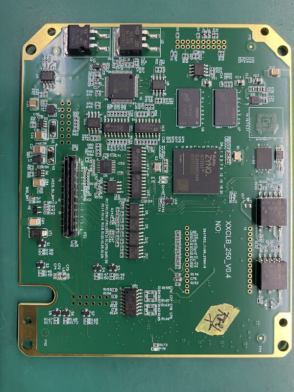
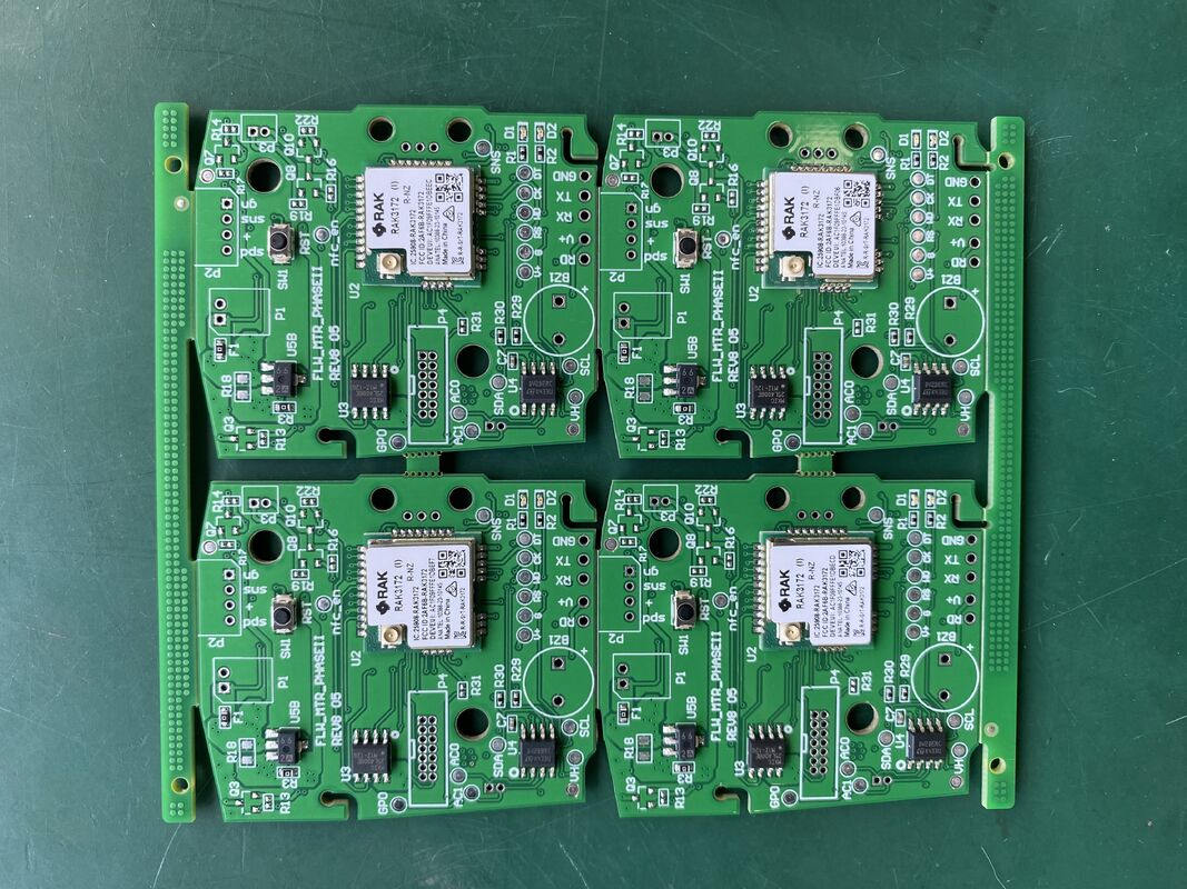
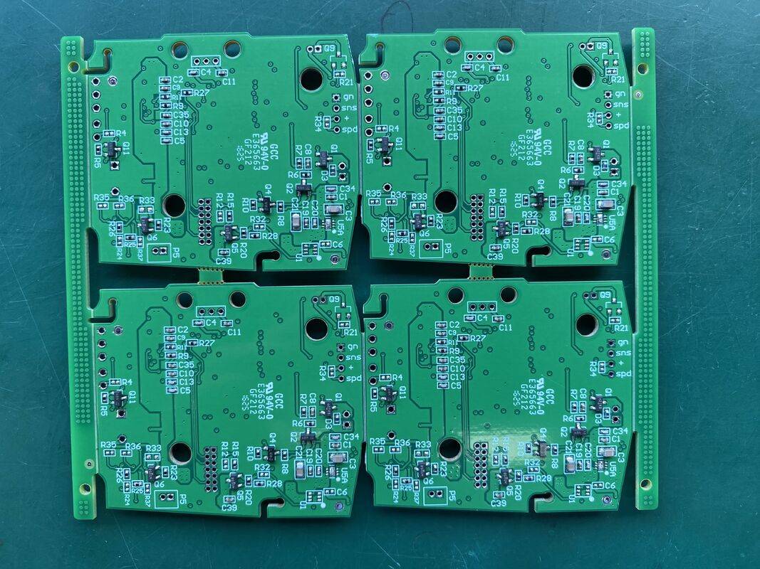
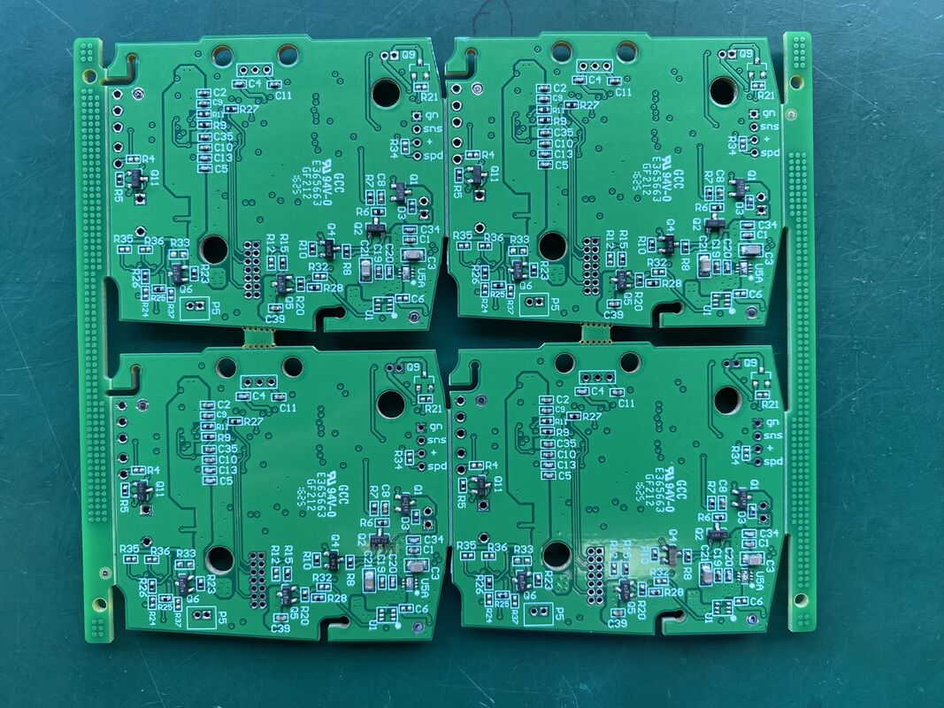
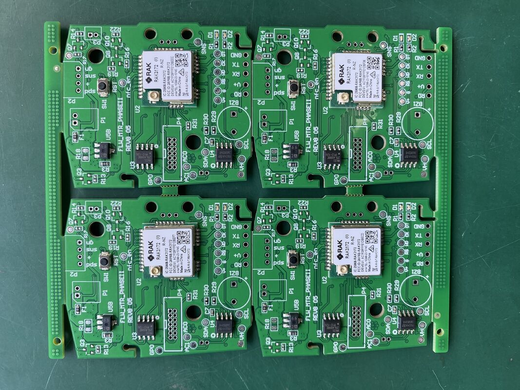
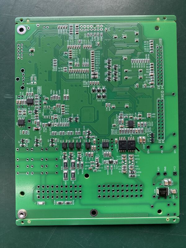
Η συναρμολόγηση PCB επικοινωνίας είναι ένα εξαιρετικά εξειδικευμένο προϊόν που έχει σχεδιαστεί για να ανταποκρίνεται στις αυστηρές απαιτήσεις της σύγχρονης υποδομής επικοινωνίας.Ως κατασκευαστής που δεσμεύεται να παρέχει ανώτερη ποιότητα και αξιοπιστία, χρησιμοποιούμε προηγμένη τεχνολογία PCB HDI (High-Density Interconnect) για να εξασφαλίσουμε εξαιρετική απόδοση και συμπαγές σχεδιασμό.Τα HDI PCB είναι γνωστά για την ικανότητά τους να υποστηρίζουν τη μετάδοση σήματος υψηλής ταχύτητας και την αυξημένη πυκνότητα κυκλώματος, καθιστώντας τους ιδανικούς για εφαρμογές επικοινωνίας όπου ο χώρος και η αποτελεσματικότητα είναι πρωταρχικά.
Ένα από τα πιο σημαντικά χαρακτηριστικά της ομάδας PCB επικοινωνίας είναι η δυνατότητα προσαρμογής.προσφέρουμε προσαρμοσμένες λύσεις για να ανταποκριθούμε στις ειδικές ανάγκες των πελατώνΕίτε πρόκειται για την προσαρμογή του μεγέθους της πλακέτας, τον αριθμό των στρωμάτων, ή την ενσωμάτωση εξειδικευμένων εξαρτημάτων, η διαδικασία κατασκευής μας είναι αρκετά ευέλικτη για να φιλοξενήσει μοναδικές προδιαγραφές,διασφάλιση ότι το τελικό προϊόν ταιριάζει απόλυτα στην προβλεπόμενη εφαρμογή.
Οι διαθέσιμες επιλογές τελικής επιφάνειας πλακών PCB για αυτή τη συναρμολόγηση περιλαμβάνουν ENIG (Electroless Nickel Immersion Gold) και HASL χωρίς μόλυβδο (Hot Air Solder Leveling).Η τελική επεξεργασία ENIG παρέχει εξαιρετική επίπεδη επιφάνεια, ανώτερη συγκολλησιμότητα και ενισχυμένη αντοχή στη διάβρωση, η οποία είναι κρίσιμη για τη διατήρηση της μακροπρόθεσμης αξιοπιστίας των συσκευών επικοινωνίας.Η φινίρισμα HASL χωρίς μόλυβδο ευθυγραμμίζεται με τα περιβαλλοντικά και κανονιστικά πρότυπα, προσφέροντας παράλληλα μια οικονομικά αποδοτική λύση χωρίς να διακυβεύεται η λειτουργικότηταΟι δύο μέθοδοι τελικής επεξεργασίας εξασφαλίζουν ότι η συναρμολόγηση PCB πληροί τα υψηλότερα πρότυπα ποιότητας που απαιτούνται στη βιομηχανία επικοινωνιών.
Η ενσωμάτωση πολλαπλών τύπων μέσω οπών, τυφλών και θαμμένων διαδρόμων, αυτή η συναρμολόγηση PCB υποστηρίζει σύνθετα σχέδια κυκλωμάτων με βελτιωμένη ηλεκτρική απόδοση και βελτιστοποίηση του χώρου.Μέσα από τα οπίσθια σωληνάρια παρέχουν ισχυρές μηχανικές συνδέσεις και αξιόπιστες ηλεκτρικές οδούς, ενώ οι τυφλοί και οι θαμμένοι σωλήνες επιτρέπουν πυκνή διασύνδεση μεταξύ των εσωτερικών στρωμάτων χωρίς να καταλαμβάνουν επιφανειακό χώρο.Αυτή η διαμόρφωση πολλαπλών διαύλων ενισχύει τη συνολική ακεραιότητα και τη λειτουργικότητα του PCB επικοινωνίας, διασφαλίζοντας ότι μπορεί να χειρίζεται σήματα υψηλής συχνότητας και να διατηρεί την ακεραιότητα του σήματος.
Η συμμόρφωση με αυστηρά πρότυπα ποιότητας είναι χαρακτηριστικό της διαδικασίας παραγωγής PCB.εγγύηση ότι το προϊόν δεν περιέχει επιβλαβείς ουσίες όπως μόλυβδοΗ συμμόρφωση αυτή όχι μόνο καθιστά το προϊόν φιλικό προς το περιβάλλον, αλλά εξασφαλίζει επίσης τη συμβατότητα με τους κανονισμούς της παγκόσμιας αγοράς,παρέχοντας στους πελάτες ηρεμία όσον αφορά την ασφάλεια και τη βιωσιμότητα.
Σχεδιασμένη ειδικά για εφαρμογές εντός της υποδομής επικοινωνίας, αυτή η σύνθεση PCB διαδραματίζει κρίσιμο ρόλο στη δυνατότητα απρόσκοπτης μετάδοσης δεδομένων και συνδεσιμότητας.Είτε χρησιμοποιείται σε εξοπλισμό δικτύωσης είτε όχι, σταθμούς βάσης ή μονάδες επικοινωνίας, το προϊόν υποστηρίζει αξιόπιστη λειτουργία υπό απαιτητικές συνθήκες.Η ενσωμάτωση χαρακτηριστικών προστασίας από υπερχείλιση στο σχεδιασμό PCB βοηθά στην προστασία ευαίσθητων ηλεκτρονικών εξαρτημάτων από τις αυξήσεις τάσης και τις παροδικές υπερχείλιεςΗ προστασία αυτή βελτιώνει την αντοχή και τη μακροζωία του συγκροτήματος, μειώνοντας τον χρόνο στάσης λειτουργίας και το κόστος συντήρησης.
Ως ένας αξιόπιστος κατασκευαστής, δίνουμε προτεραιότητα στην ενσωμάτωση της τεχνολογίας αιχμής με σχολαστικό έλεγχο ποιότητας για να παραδώσουμε Συνεδριάσεις PCB Επικοινωνίας που πληρούν και ξεπερνούν τις προσδοκίες της βιομηχανίας.Η συνολική προσέγγισή μας, από την προσαρμογή του σχεδιασμού έως την προηγμένη τελική επεξεργασία της επιφάνειας και την εφαρμογή πολλαπλών διαύλων, διασφαλίζει ότι κάθε συναρμολόγιο είναι βελτιστοποιημένο για τις καλύτερες επιδόσεις στις εφαρμογές υποδομών επικοινωνιών.Η ενσωμάτωση της προστασίας από τις υπερεχύσεις προσθέτει περαιτέρω αξία, ενισχύοντας την αξιοπιστία του συστήματος και προστατεύοντας τον κρίσιμο εξοπλισμό επικοινωνίας.
Συνοπτικά, η συναρμολόγηση PCB επικοινωνίας είναι ένα ευπροσάρμοστο, υψηλής απόδοσης προϊόν προσαρμοσμένο στις εξελισσόμενες ανάγκες του τομέα των επικοινωνιών.Προσαρμόσιμες επιλογές σχεδιασμού, υψηλής ποιότητας επιφάνειας με ENIG και HASL χωρίς μόλυβδο και διαμορφώσεις πολλαπλών διαύλων, αποτελεί μια ισχυρή λύση για σύνθετα κυκλώματα επικοινωνίας.Η συμμόρφωση με τα πρότυπα ROHS και η ενσωματωμένη προστασία από υπερεχύσεις υπογραμμίζουν την ποιότητα και την αξιοπιστία του, καθιστώντας το απαραίτητο συστατικό της σύγχρονης υποδομής επικοινωνιών.Η συνεργασία με έναν έμπειρο κατασκευαστή διασφαλίζει ότι οι πελάτες λαμβάνουν ένα προϊόν σχεδιασμένο για την αριστεία και σχεδιασμένο για να υποστηρίζει τις κρίσιμες απαιτήσεις του σημερινού συνδεδεμένου κόσμου.
Χαρακτηριστικά:
- Ονομασία προϊόντος: Συνδυασμός PCB επικοινωνίας
- Πεδίο εφαρμογής: 5G επικοινωνία
- Πίνακες PCB επικοινωνίας: υψηλή Tg170 και υψηλή Tg180
- Σύστημα ποιότητας PCB: Συμμόρφωση με το ROHS
- Ελέγχος αντίστασης: Ναι
- Χρωματικές επιλογές μάσκας συγκόλλησης: Μπλε, πράσινο κλπ.
- Σχεδιασμένο από αξιόπιστο κατασκευαστή που ειδικεύεται στις υποδομές επικοινωνιών
- Ο κατασκευαστής εξασφαλίζει υψηλά πρότυπα ποιότητας για βέλτιστη απόδοση στις συσκευές επικοινωνίας
Τεχνικές παραμέτρους:
| Ονομασία του προϊόντος |
Συνέλευση PCB επικοινωνίας |
| Τάγματα PCB |
6 στρώσεις |
| Προσαρμοσμένο |
- Ναι, ναι. |
| Έλεγχος αντίστασης |
- Ναι, ναι. |
| Διάμετρος τρύπας |
0.1 mm |
| Χρώμα μάσκας συγκόλλησης |
Μπλε, πράσινο, κλπ. |
| Πίνακας PCB |
HDI PCB |
| Πεδίο εφαρμογής |
Επικοινωνία 5G |
| Τελεία επιφάνειας |
ENIG, HASL Χωρίς μόλυβδο |
| Εξωτερική συσκευασία |
Καρτόνι |
| Ειδικά χαρακτηριστικά |
Σημαντικό ρεύμα, προστασία από υπερχείλιση, παχύ χαλκό |
Εφαρμογές:
Η συναρμολόγηση PCB επικοινωνίας είναι ένα κρίσιμο συστατικό που έχει σχεδιαστεί ειδικά για τις προηγμένες απαιτήσεις της βιομηχανίας επικοινωνιών 5G.Κατανοούμε τις αυστηρές απαιτήσεις που έρχονται με τα σύγχρονα συστήματα επικοινωνίας.Το προϊόν αυτό έχει σχεδιαστεί με ακριβή έλεγχο παρεμπόδισης για να διασφαλιστεί η βέλτιστη ακεραιότητα του σήματος, η οποία είναι απαραίτητη για τις υψηλής συχνότητας μεταδόσεις που χαρακτηρίζουν τα δίκτυα 5G.Η ικανότητα διατήρησης σταθερής αντίστασης σε όλο το πλαίσιο μειώνει την απώλεια σήματος και τις παρεμβολές, βελτιώνοντας έτσι τη συνολική απόδοση της επικοινωνίας.
Με ευπροσάρμοστο εύρος πάχους πλάκας 0,2-6 mm, η Συνέλευση PCB Επικοινωνίας ανταποκρίνεται σε διάφορες απαιτήσεις σχεδιασμού,καθιστώντας το κατάλληλο για ένα ευρύ φάσμα εφαρμογών εντός της υποδομής 5GΕίτε χρησιμοποιείται σε συμπαγείς κινητές συσκευές, σταθμούς βάσης, είτε σε δρομολογητές δικτύου,η ευελιξία στο πάχος επιτρέπει στους σχεδιαστές να βελτιστοποιούν τις φυσικές και ηλεκτρικές ιδιότητες σύμφωνα με τις ειδικές ανάγκεςΟι επιλογές τελικής επιφάνειας, συμπεριλαμβανομένων των ENIG (Electroless Nickel Immersion Gold) και των HASL (Hot Air Solder Leveling) χωρίς μόλυβδο, παρέχουν εξαιρετική συγκόλληση και αντοχή.διασφάλιση αξιόπιστων συνδέσεων ακόμη και σε συνθήκες ισχυρού ρεύματος που συχνά συναντώνται στους εξοπλισμούς επικοινωνίας.
Αυτή η ανθεκτική συναρμολόγηση PCB είναι ιδανική για σενάρια όπου η επικοινωνία υψηλών επιδόσεων και η αξιοπιστία είναι πρωταρχικές.Χρησιμοποιείται ευρέως σε εφαρμογές υψηλού ρεύματος σε σταθμούς βάσης 5G, όπου η σταθερή παροχή ισχύος και η ελάχιστη στρέβλωση του σήματος είναι κρίσιμεςΟι κατασκευαστές που εφαρμόζουν αυτό το προϊόν επωφελούνται από την ανώτερη ποιότητα κατασκευής και τις σταθερές επιδόσεις του, γεγονός που μεταφράζεται σε μεγαλύτερη διάρκεια ζωής και μειωμένα κόστη συντήρησης.Η συμβατότητα της πλακέτας με διάφορες επιφάνειες επιφάνειας της επιτρέπει να αντέχει σε σκληρές περιβαλλοντικές συνθήκες., καθιστώντας το κατάλληλο για εξωτερικούς πύργους επικοινωνίας και βιομηχανικές συσκευές επικοινωνίας.
Συνοπτικά, η συναρμολόγηση PCB επικοινωνίας ξεχωρίζει ως προτιμώμενη επιλογή για τους κατασκευαστές που εστιάζουν στην παροχή πρωτοποριακών λύσεων επικοινωνίας 5G.Δυνατότητα προσαρμογής πάχους πλάκαςΤο υλικό αυτό, το οποίο χρησιμοποιείται σε σενάρια με έντονο ρεύμα ή σε συμπαγείς συσκευές, μπορεί να χρησιμοποιηθεί για την κατασκευή ηλεκτρικών συσκευών.το προϊόν αυτό υποστηρίζει την απρόσκοπτη μετάδοση δεδομένων, επιτρέποντας τη δημιουργία της επόμενης γενιάς δικτύων επικοινωνίας υψηλής ταχύτητας και χαμηλής καθυστέρησης παγκοσμίως.
Προσαρμογή:
Το προϊόν μας για την συναρμολόγηση PCB επικοινωνίας προσφέρει ολοκληρωμένες υπηρεσίες προσαρμογής για την κάλυψη των ειδικών αναγκών των κατασκευαστών.Ειδικευόμαστε σε υψηλής ποιότητας HDI πλακέτες PCB που εξασφαλίζουν ανώτερη απόδοση και αξιοπιστίαΟι διαθέσιμες επιλογές τελικής επιφάνειας περιλαμβάνουν ENIG και HASL Lead Free, παρέχοντας εξαιρετική συγκολλησιμότητα και αντοχή για τις συγκεντρώσεις σας.
Ακολουθούμε αυστηρά το σύστημα ποιότητας PCB ROHS, διασφαλίζοντας ότι όλα τα υλικά και οι διαδικασίες συμμορφώνονται με τα πρότυπα περιβάλλοντος και ασφάλειας.Τα χρώματα μάσκας συγκόλλησης μας είναι διαθέσιμα σε διάφορες επιλογές όπως μπλε, πράσινο, και άλλα για να ταιριάζει με τις προτιμήσεις σχεδιασμού σας.
Με ελάχιστη διάμετρο τρύπας 0,1mm, η διαδικασία κατασκευής μας υποστηρίζει πολύπλοκα και ακριβή σχέδια κυκλωμάτων, ιδανικά για προηγμένες εφαρμογές επικοινωνίας.Επίσης, ενσωματώνουμε χαρακτηριστικά προστασίας από υπερτάσεις για να ενισχύσουμε την ασφάλεια και τη μακροζωία των συσκευών επικοινωνίας σας..
Επιλέξτε τις υπηρεσίες προσαρμογής της συναρμογής PCB επικοινωνίας μας για αξιόπιστες λύσεις κατασκευής προσαρμοσμένες στις τεχνικές σας απαιτήσεις και τα πρότυπα του κλάδου.
Υποστήριξη και υπηρεσίες:
Το προϊόν μας για την συναρμολόγηση PCB επικοινωνίας υποστηρίζεται από μια εξειδικευμένη ομάδα τεχνικής υποστήριξης που δεσμεύεται να εξασφαλίζει βέλτιστη απόδοση και αξιοπιστία.Προσφέρουμε ολοκληρωμένες υπηρεσίες, συμπεριλαμβανομένης της συμβουλευτικής σχεδιασμού, επίλυση προβλημάτων συναρμολόγησης και δοκιμές μετά την παραγωγή για την κάλυψη των ειδικών αναγκών των συστημάτων επικοινωνίας σας.
Οι ειδικοί μας βοηθούν με την επιλογή των εξαρτημάτων, τη βελτιστοποίηση της διάταξης και την ανάλυση της ακεραιότητας του σήματος για να βελτιώσουν τη λειτουργικότητα των συνόλων PCB σας.Παρέχουμε επίσης υποστήριξη ενσωμάτωσης firmware και επαλήθευση συμβατότητας για να εξορθολογίσει την διαδικασία ανάπτυξης σας.
Επιπλέον, προσφέρουμε υπηρεσίες επισκευής και ανακαίνισης για να παρατείνουμε τη διάρκεια ζωής των επικοινωνιακών PCBs σας,μαζί με τακτικά προγράμματα συντήρησης που έχουν σχεδιαστεί για την πρόληψη των διακοπών και την εξασφάλιση της συνεπούς λειτουργίας.
Η δέσμευσή μας για την ποιότητα υποστηρίζεται από λεπτομερή τεκμηρίωση και εγχειρίδια χρήστη,καθώς και εκπαιδευτικές συνεδρίες για την ενδυνάμωση της ομάδας σας με τη γνώση για τη συντήρηση και την αντιμετώπιση προβλημάτων των συναρμολογήσεων αποτελεσματικά.
Συσκευή και αποστολή:
Κάθε συναρμολόγιο τοποθετείται σε αντιστατικές σακούλες για να αποφευχθεί η ηλεκτροστατική βλάβη.ακολουθείται από μαξιλαρισμένα υλικά συσκευασίας για την απορρόφηση συγκρούσεων και δονήσεων.
Τα συσκευασμένα προϊόντα στη συνέχεια συσκευάζονται με ασφάλεια σε ανθεκτικά, κυματοειδή κουτιά από χαρτόνι, που έχουν σχεδιαστεί για να αντέχουν σε σκληρό χειρισμό.Χρησιμοποιούνται πρόσθετοι εσωτερικοί διαχωριστές και επένδυση για τη διατήρηση κάθε συνόλου PCB χωριστού και ασφαλούς..
Προσφέρουμε διάφορες επιλογές αποστολής για να ανταποκριθούμε στις απαιτήσεις παράδοσης σας, συμπεριλαμβανομένων των τυποποιημένων, ταχείων και εμπορευματικών υπηρεσιών.Όλες οι αποστολές παρακολουθούνται και ασφαλίζονται για να εγγυηθούν την έγκαιρη και ασφαλή παράδοση..
Πριν από την αποστολή, κάθε σύνολο PCB επικοινωνίας υποβάλλεται σε λεπτομερή επιθεώρηση ποιότητας για να διασφαλιστεί ότι πληροί όλες τις τεχνικές προδιαγραφές και τις απαιτήσεις των πελατών.
Η ομάδα εφοδιασμού μας συντονίζεται στενά με αξιόπιστους μεταφορείς για να παρέχει απρόσκοπτη παγκόσμια αποστολή, διασφαλίζοντας ότι τα προϊόντα σας φτάνουν εγκαίρως και σε τέλεια κατάσταση.


 Το μήνυμά σας πρέπει να αποτελείται από 20-3.000 χαρακτήρες!